Problem
Develop a block diagram and an ASMD chart for a digital circuit that multiplies two binary numbers by the repeated-addition method. For example, to multiply 5 × 4, the digital system evaluates the product by adding the multiplicand four times: 5 + 5 + 5 + 5 = 20. Design the circuit. Let the multiplicand be in register BR, the multiplier in register AR, and the product in register PR . An adder circuit adds the contents of BR to PR . A zero-detection signal indicates whether AR is 0. Write and verify a Verilog behavioral model of the circuit.
Step-by-step solution
Step 1 of 10
The block diagram of a digital circuit which multiplies two binary numbers by the repeated –addition method is shown below: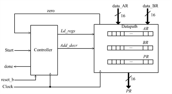
Comment Step 2 of 10
The block diagram shown above consists of a controller and a datapath unit. The controller controls the working of the digital circuit. The control unit produces some control signals as its output which acts as the input to the datapath unit.The datapath unit consists of three registers AR, BR, PR. The multiplicand is stored in the register BR, the multiplier is stored in the register AR, and the product is stored in the register PR. The adder circuit will add the contents of BR to PR. And a Zero – detection signal indicates whether AR is 0.Comment Step 3 of 10
The ASMD chart for the digital circuit is shown below: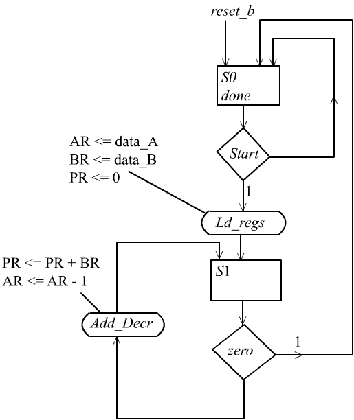
Comment Step 4 of 10
The initial state of the circuit is S0. If the start is equal to 1, then multiplicand will store on BR register, the multiplier will store in the register AR and the PR becomes 0.Then go to S1 state. After that go to zero for detecting whether the content in the AR is zero. If AR is equal to zero (zero = 1), go back to the initial state. Otherwise, go to Add_Decr, where the PR is added with BR and is stored in PR. And the content of the AR is decremented by 1. After that go to S1.The controller unit of the digital circuit is shown below: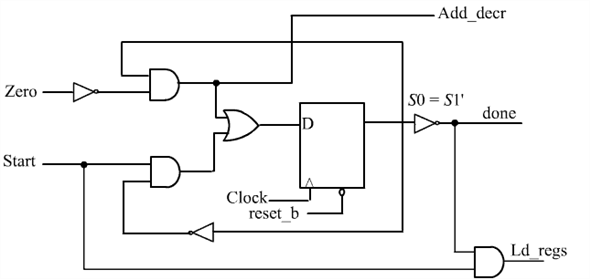
Comment Step 5 of 10
The controller consists of a D flip-flop. The clock and reset inputs are given to it. The Start and Zero signal are the input signals. The Add_decr and Ld_regs are the output signals and it is given as input to the data path unit. S0 is the initial state. The flip-flop will reset at the initial state.Only when Start is equal to one, the output Ld_regs produces.Comment Step 6 of 10
The internal architecture of the AR register in the datapath unit is shown below: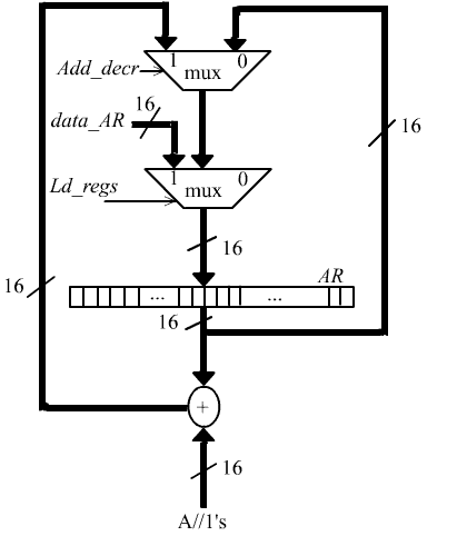
Comment Step 7 of 10
The internal architecture of the AR register consists of a register to hold the multiplier value. And also a single width parallel adder is there to implement the operation of decrementing the content of AR.Comment Step 8 of 10
The internal architecture of the BR and PR of the datapath unit is shown below: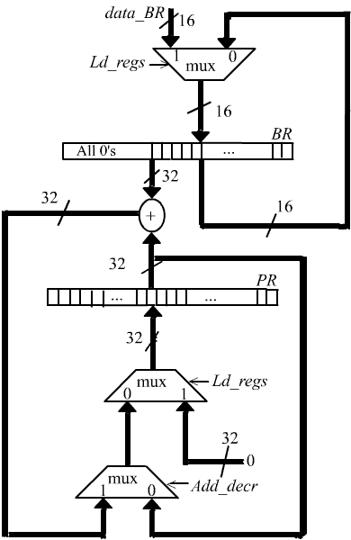 The internal architecture of the BR and PR consists of a double-width register to hold the product (PR), and another register BR to store the multiplicand value. There is a double – width parallel adder for adding the contents of BR and PR.
Comment Step 9 of 10
The behavioral model for the circuit is shown below:module digi_ckt (output [15: 0] PR, output done,input [7: 0] data_AR, data_BR, input start, clock, reset_b);Controller_ digi_ckt M0 (done, Ld_regs, Add_decr, start, zero, clock, reset_b);Datapath_ digi_ckt M1 (PR, zero, data_AR, data_BR, Ld_regs, Add_decr, clock, reset_b);endmodulemodule Controller_ digi_ckt (output done, output reg Ld_regs, Add_decr, input start, zero, clock, reset_b);parameter s0 = 1'b0, s1 = 1'b1;reg state, next_state;assign done = (state == s0);always @ (posedge clock, negedge reset_b)if (!reset_b) state <= s0; else state <= next_state;always @ (state, start, zero) beginLd_regs = 0;Add_decr = 0;case (state)s0: if (start) begin Ld_regs = 1; next_state = s1; ends1: if (zero) next_state = s0; else begin next_state = s1; Add_decr = 1; enddefault: next_state = s0;endcaseendendmodulemodule Register_32 (output [31: 0] data_out, input [31: 0] data_in, input clock, reset_b);Register_8 M3 (data_out [31: 24] , data_in [31: 24], clock, reset_b);Register_8 M2 (data_out [23: 16] , data_in [23: 16], clock, reset_b);Register_8 M1 (data_out [15: 8] , data_in [15: 8], clock, reset_b);Register_8 M0 (data_out [7: 0] , data_in [7: 0], clock, reset_b);endmodulemodule Register_16 (output [15: 0] data_out, input [15: 0] data_in, input clock, reset_b);Register_8 M1 (data_out [15: 8] , data_in [15: 8], clock, reset_b);Register_8 M0 (data_out [7: 0] , data_in [7: 0], clock, reset_b);endmodulemodule Register_8 (output [7: 0] data_out, input [7: 0] data_in, input clock, reset_b);D_flop M7 (data_out[7] data_in[7], clock, reset_b);D_flop M6 (data_out[6] data_in[6], clock, reset_b);D_flop M5 (data_out[5] data_in[5], clock, reset_b);D_flop M4 (data_out[4] data_in[4], clock, reset_b);D_flop M3 (data_out[3] data_in[3], clock, reset_b);D_flop M2 (data_out[2] data_in[2], clock, reset_b);D_flop M1 (data_out[1] data_in[1], clock, reset_b);D_flop M0 (data_out[0] data_in[0], clock, reset_b);endmodulemodule Adder_32 (output c_out, output [31: 0] sum, input [31: 0] a, b);assign {c_out, sum} = a + b;endmodulemodule Adder_16 (output c_out, output [15: 0] sum, input [15: 0] a, b);assign {c_out, sum} = a + b;endmodulemodule D_flop (output q, input data, clock, reset_b);always @ (posedge clock, negedge reset_b)if (!reset_b) q <= 0; else q <= data;endmodulemodule Datapath_ digi_ckt (output reg [15: 0] PR, output zero,input [7: 0] data_AR, data_BR, input Ld_regs, Add_decr, clock, reset_b);reg [7: 0] AR, BR;assign zero = ~( | AR);always @ (posedge clock, negedge reset_b)if (!reset_b) begin AR <= 8'b0; BR <= 8'b0; PR <= 16'b0; endelse beginif (Ld_regs) begin AR <= data_AR; BR <= data_BR; PR <= 0; endelse if (Add_decr) begin PR <= PR + BR; AR <= AR -1; endendendmodulemodule t_ digi_ckt;wire done;wire [15: 0] PR;reg [7: 0] data_AR, data_BR;reg start, clock, reset_b;digi_ckt _STR M0 (PR, done, data_AR, data_BR, start, clock, reset_b);initial #500 $finish;initial begin clock = 0; forever #5 clock = ~clock; endinitial forkreset_b = 0;#12 reset_b = 1;#40 reset_b = 0;#42 reset_b = 1;#90 reset_b = 1;#92 reset_b = 1;joininitial fork#20 start = 1;#30 start = 0;#40 start = 1;#50 start = 0;#120 start = 1;#120 start = 0;joininitial forkdata_AR = 8'd5; // AR > 0data_BR = 8'd20;#80 data_AR = 8'd3;#80 data_BR = 8'd9;#100 data_AR = 8'd4;#100 data_BR = 8'd9;joinendmoduleComment Step 10 of 10
The simulation output waveform for the above behavioral description is shown below: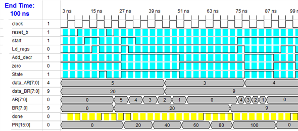
Comment
